[

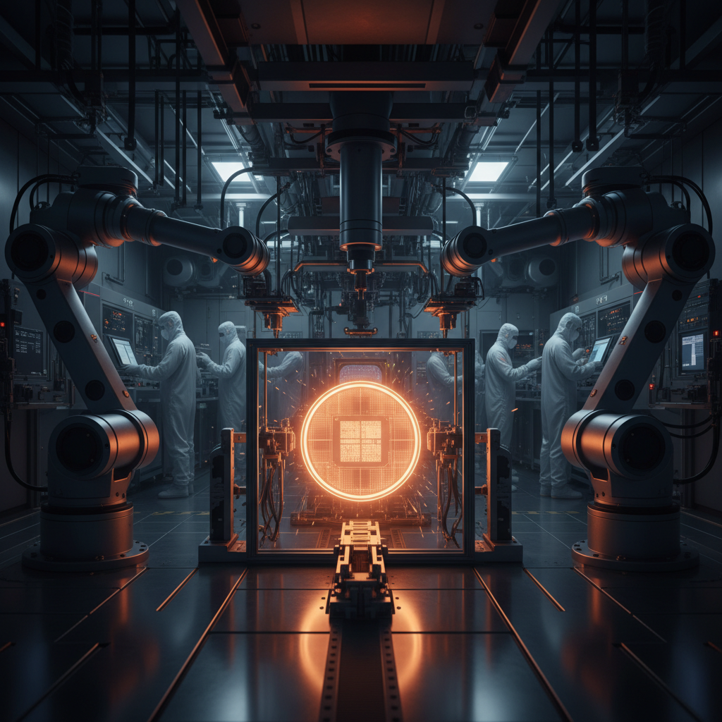
Nvidia](https://www.amazon.sg/s?k=nvidia+gpu&tag=aiinasia-22) Unveils Feynman Architecture and Ships Vera Rubin Samples at GTC 2026 Jensen Huang used Nvidia's annual GTC conference on 16 March to pull back the curtain on Feynman, the company's next-generation AI chip architecture slated for 2028. Feynman will feature an eighth-generation NVSwitch, a new CPU codenamed Rosa, and a 204Tbps network fabric designed for massive-scale inference clusters. Huang also confirmed that Vera Rubin, the platform succeeding Blackwell, has begun shipping samples to customers ahead of full production in the second half of this year. Nvidia claims Vera Rubin delivers five times the inference performance and ten times lower cost per token than Blackwell.
Why it matters for Asia
Feynman will be manufactured on TSMC's 1.6nm A16 process, marking Nvidia's first use of a sub-2nm node and deepening its dependence on Taiwan's chip fabrication ecosystem. Samsung Electronics and SK hynix are confirmed as key HBM4 memory suppliers for the Vera Rubin platform, cementing South Korea's role in the AI silicon supply chain. For enterprise buyers across Asia, Vera Rubin's inference economics could materially lower the cost of deploying large language models at scale.^